Optimizing DLC Coatings for Hardness and Low Friction on Nuclear Valve Stems
Aug 24, 2025
Abstract: This study investigates the effects of varying deposition process parameters, such as workpiece bias voltage and W-doped target power, on the performance of DLC coatings applied to valve stems. The chemical composition and structure of the coatings were analyzed using Raman spectroscopy, and their mechanical properties were evaluated through nanoindentation and microscratch testing. Tribological performance was assessed through friction and wear testing. The results indicate that DLC coatings deposited at a workpiece bias voltage of 1200 V exhibit higher hardness and lower wear rates. In contrast, W-doped DLC coatings exhibited stronger adhesion but lower hardness and higher wear rates. These findings offer valuable guidance for optimizing the deposition process to produce high-hardness, low-friction DLC coatings suitable for nuclear power applications.
Valves in nuclear power plants operate under long-term, non-lubricated conditions and are exposed to corrosive media, abrasion, vibration, and other harsh factors, which make them highly susceptible to wear. As a critical valve component, the stem functions both as a moving, load-bearing part and as a sealing element. Excessive wear can significantly compromise its performance and reduce its service life. The data indicate that insufficient surface wear resistance is the primary cause of component failure. Therefore, developing advanced wear-resistant coatings is essential for enhancing the durability of key components in nuclear power systems, providing significant economic and safety benefits.
Diamond-like carbon (DLC) is a highly effective protective coating, renowned for its exceptional hardness, low friction coefficient, and excellent wear resistance. The mechanical and tribological properties of DLC coatings are closely related to their atomic carbon bonding structure—specifically, the ratio of sp² (graphite-like) to sp³ (diamond-like) hybridized carbon atoms. In addition, the incorporation of doping elements can modify the film’s structure and the strength of internal chemical bonds, thereby influencing its mechanical and tribological performance. Currently, physical vapor deposition (PVD) is the most widely used method for preparing DLC coatings. Common PVD techniques include evaporation, magnetron sputtering, and arc discharge sputtering. Among these, magnetron sputtering has become the predominant technology due to its high deposition rate, uniform film thickness, capability for multi-material deposition, and precise process control. Controlling deposition parameters plays a crucial role in determining the properties of DLC coatings, especially their mechanical strength and resistance to friction and wear. This study employs magnetron sputtering to investigate the effects of various process parameters—including workpiece bias voltage, W target power, and tungsten (W) doping—on the mechanical and tribological properties of DLC coatings. These findings aim to provide a foundation for future research on multilayer coating processes to develop DLC coatings with enhanced overall performance.
This study employed a Star Arc Diamant 340 magnetron sputtering system for coating deposition, incorporating ion beam equipment during the preparation process. In a vacuum chamber, magnetic and electric fields were applied to ionize argon gas, which was then accelerated to bombard the surface of the target pellets. This process ejected solid particles that were subsequently deposited onto the surface of 17-4PH stainless steel substrates to form thin films. All substrates were first cleaned by argon ion etching at an Ar gas flow rate of 50 SCCM, a workpiece bias voltage of 1200 V, a duty cycle of 25%, and an ion beam voltage of 1700 V. Following this, a chromium (Cr) bonding layer was deposited to match the thermal expansion coefficients of the substrate and the coating. The Cr layer was deposited under an Ar flow rate of 45 SCCM, a bias voltage of 200 V, a duty cycle of 70%, and a Cr target power of 1500 W. Two types of DLC coating samples were then deposited on the Cr bonding layer. The first type was prepared by varying the workpiece bias voltage at a CH₄ gas flow rate of 100 SCCM and a constant ion beam voltage of 1400 V, resulting in Samples 11, 12, and 13. The second type involved depositing a tungsten (W) bonding layer under an Ar gas flow rate of 45 SCCM, a bias voltage of 200 V, a duty cycle of 70%, and a W target power of 1500 W. Subsequently, W-doped DLC (W-DLC) coatings—Samples 21, 22, and 23—were deposited by adjusting the workpiece bias voltage and W target power, using a mixed gas flow of 25 SCCM C₂H₂ and 40 SCCM Ar. The specific process parameters are listed in Table 1, and the coating structures are illustrated in Figure 2.
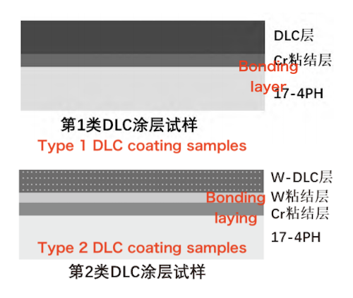
Figure 2. Schematic diagram of DLC composite coating structures obtained under different process conditions
Surface morphology, cross-sectional structure, and elemental distribution were analyzed using a Zeiss Sigma 300 field emission scanning electron microscope (FE-SEM) equipped with energy-dispersive X-ray spectroscopy (EDS). A Horiba HR800 confocal Raman spectrometer was used to characterize the chemical bonding structures of the DLC and W-DLC coatings. Friction and wear performance were evaluated using a self-developed fretting wear testing machine. The hardness of the coatings and substrate was measured using both a KLAG200 nanoindenter and a CSM Instruments DRSX 70055 system. Adhesion between the coating and substrate was assessed using a CalibrationKit RSX scratch tester.
Table 2 presents the surface elemental composition of each DLC composite coating. The first group of samples (Samples 11–13) consists solely of carbon on the surface, indicating pure DLC coatings without the incorporation of additional elements. In contrast, the second group of samples (Samples 21–23) contains both carbon and tungsten, confirming successful tungsten doping in the W-DLC coatings.
Table 1. Sample Numbers
|
Sample No. |
Coating Type |
|
11 |
DLC |
|
12 |
DLC |
|
13 |
DLC |
|
21 |
W-DLC |
|
22 |
W-DLC |
|
23 |
W-DLC |
Table 2. Surface Elemental Composition of DLC Composite Coatings (%)
|
Sample No. |
C |
W |
Ar |
|
11 |
100.0 |
– |
– |
|
12 |
100.0 |
– |
– |
|
13 |
100.0 |
– |
– |
|
21 |
37.7 |
60.7 |
1.6 |
|
22 |
38.1 |
59.6 |
2.3 |
|
23 |
37.3 |
61.6 |
1.1 |
Figures 3(a)–(c) display the surface morphologies of Samples 11, 12, and 13 (first coating type), while Figures 3(d)–(f) correspond to the surface morphologies of Samples 21, 22, and 23 (second coating type), respectively. Samples 11, 12, and 13 were deposited under workpiece bias voltages of 800 V, 1200 V, and 1600 V, respectively. The results show that increasing the bias voltage leads to smaller particle sizes and a denser surface morphology. This is primarily because a higher bias voltage increases the kinetic energy of incident particles, thereby enhancing the mobility of surface atoms and promoting denser film growth. However, the surface particle sizes of Samples 11 and 13 are relatively larger. For Sample 11, this is attributed to the low bias voltage, which leads to a reduced deposition rate and a more porous film structure. In Sample 11, the larger particle size is attributed to the low bias voltage, which leads to a reduced deposition rate and a more porous film structure. In contrast, the large particles observed in Sample 13 are attributed to the excessively high bias voltage, which causes intense sputtering and promotes particle agglomeration.
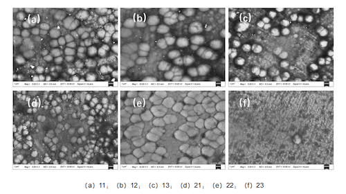
Figure 3. SEM surface morphologies of DLC composite coatings: (a) 11; (b) 12; (c) 13; (d) 21; (e) 22; (f) 23
Figures 3(d), (e), and (f) display the surface morphologies of the W-DLC coatings (Samples 21–23), which were deposited under different W target powers and workpiece bias voltages. An increase in either the W target power or the workpiece bias voltage results in a higher deposition rate. Compared to Sample 21, the surfaces of Samples 22 and 23 are noticeably denser and more uniform. In particular, Sample 23 (Figure 3(f)) exhibits a finer grain structure, with the smallest average grain size among the three samples. Additionally, due to the lower deposition rate, both Samples 11 and 21 exhibit void-like defects, which are likely caused by uneven or insufficient film thickness.
Figures 4(a)–(c) depict the cross-sectional morphologies of Samples 11, 12, and 13, while Figures 4(d)–(f) correspond to Samples 21, 22, and 23.
As shown in Figure 4, the Cr bonding layer appears as a thin, bright stripe in all samples, with overall film thicknesses remaining relatively consistent. For the first coating process, the DLC film deposited at the lowest bias voltage (800 V, Sample 11) is thinner, owing to the reduced deposition rate. While the film While the film thicknesses of Samples 12 and 13 are similar, Sample 13 exhibits a denser microstructure with fewer internal defects. For the second coating process (W-DLC), increasing the bias voltage significantly increases the thickness of the DLC film. In contrast, increasing the W target power does not significantly affect the film thickness but results in a denser film structure.
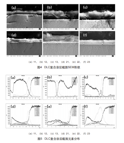
Figure 4. SEM cross-sectional morphologies of DLC composite coatings: (a) 11; (b) 12; (c) 13; (d) 21; (e) 22; (f) 23
Figure 5. Cross-sectional EDS elemental mapping of DLC composite coatings: (a) 11; (b) 12; (c) 13; (d) 21; (e) 22; (f) 23
Figures 5(a) through 5(f) present the EDS elemental distribution maps corresponding to the cross-sections of Samples 11–23. As shown in Figure 5, the bonding layers of all coatings consist of chromium (Cr), whereas the substrate material is primarily composed of iron (Fe). In the first coating structure (Samples 11–13), the surface layer consists entirely of carbon (C), with chromium (Cr) diffusion observed at the film-substrate interface. In the second coating structure (Samples 21–23), the surface layer exhibits a high tungsten (W) content, accompanied by chromium (Cr) diffusion near the interface, indicating effective bonding and elemental transition across the layers.
Figures 5(a)–(c) and 5(d)–(f) present the cross-sectional SEM-EDS elemental mapping results for the respective specimens. As shown in Figure 5, the bonding layer of all coatings comprises chromium (Cr), while the substrate is primarily composed of iron (Fe). In the first coating structure (Samples 11–13), the surface layer is composed entirely of carbon (C), with chromium (Cr) diffusion observed at the interface between the film and the substrate. In the second coating structure (Samples 21–23), a significant amount of tungsten (W) is present in the surface layer, with chromium (Cr) diffusion likewise observed near the film-substrate interface.
The relative content of sp² bonding in DLC coatings is a crucial factor affecting their mechanical properties. The sp²/sp³ ratio can be determined by Raman spectroscopy. Figure 6 shows the Raman spectra of six DLC coating samples. Deconvolution analysis was performed on the characteristic G and D peaks, and the integrated intensity ratio (I_D/I_G) was calculated. Additionally, the peak positions and full widths at half maximum (FWHM) of the D and G peaks were determined. The D peak corresponds to the C–C sp² aromatic ring structure, whereas the G peak is associated with the symmetric stretching of sp² C–C bonds within the ring. The I_D/I_G ratio generally reflects the degree of disorder in the film: a lower I_D/I_G value indicates a more ordered structure and, empirically, superior mechanical properties. The full width at half maximum of the G peak (FWHM_G) is related to the size of sp² clusters in the film—a larger FWHM_G indicates smaller sp² cluster size.
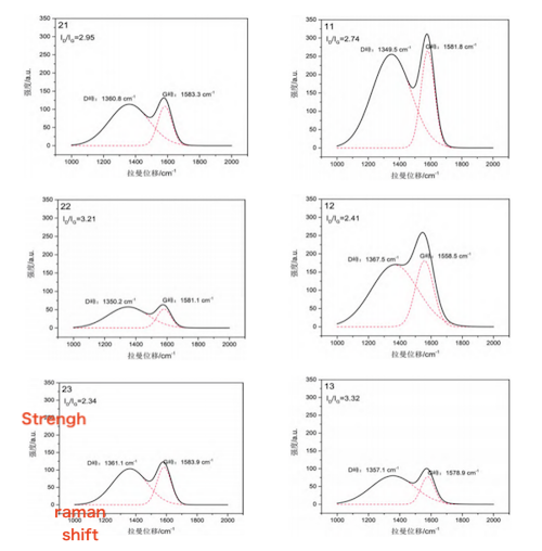
Figure 6. Raman spectra of DLC composite coatings
For the first coating type, the I_D/I_G values of the three samples initially decrease and then increase as the bias voltage rises. The DLC coating deposited at a bias voltage of 1200 V demonstrates optimal mechanical properties. Concurrently, the FWHM_G values increase initially and then decrease, suggesting that the size of the sp² clusters first diminishes and then grows with rising bias voltage. This behavior is attributed to the restructuring of carbon bonding between sp² and sp³ configurations. The mechanical properties show a positive correlation with the presence of sp³ structures. For the second coating type, the FWHM_G values of the three samples remain relatively consistent, possibly due to the introduction of tungsten (W), which reduces internal stress within the film. The presence of larger sp² clusters in these coatings may enhance film adhesion. Although the I_D/I_G values are relatively high, the mechanical properties of the W-DLC coatings are not particularly remarkable.
The mechanical properties of the coatings include adhesion, nanohardness, and elastic modulus. The key mechanical parameters for each coating are summarized in Table 3. As shown in Table 3, among all samples, Sample 12 exhibits the highest nanohardness at 25.8 GPa, while the nanohardness values of the other coatings remain below 20 GPa. According to the Raman spectroscopy results, the superior performance of Sample 12 can be attributed to its optimal sp²/sp³ bonding structure and film density.
Table 3. Mechanical properties of DLC composite coatings.
|
Sample |
Nanohardness (GPa) |
Elastic Modulus (GPa) |
H/E |
H³/E² |
Adhesion (N) |
|
11 |
12.2 |
109.2 |
0.111 |
0.151 |
28 |
|
12 |
25.8 |
223.8 |
0.115 |
0.341 |
– |
|
13 |
14.8 |
134.1 |
0.111 |
0.182 |
28 |
|
21 |
16.4 |
218.9 |
0.075 |
0.092 |
33 |
|
22 |
13.8 |
172.7 |
0.080 |
0.089 |
27 |
|
23 |
14.4 |
146.7 |
0.099 |
0.374 |
28 |
An increased sp² content in the film typically enhances hardness. Improved adhesion observed in the second coating process is mainly due to reduced internal stress in the film caused by tungsten (W) doping or alterations in process parameters. Moreover, the hardness-to-modulus ratios—H/E and H³/E²—are commonly used to evaluate a coating’s resistance to plastic deformation, which reflects its toughness. Higher values of these ratios typically indicate improved toughness. Overall, the coatings produced by the first process exhibit better toughness according to these mechanical indicators.
Table 4. Friction and wear properties of DLC composite coatings.
|
Sample |
Dynamic Friction Coefficient |
Wear Scar Depth (μm) |
Wear Rate (mm³/(N·m)) |
Coating Thickness (μm) |
|
11 |
0.066 |
–11.5 |
5.3877 × 10⁷ |
3.1 |
|
12 |
0.093 |
–1.3 |
0.0987 × 10⁷ |
6.6 |
|
13 |
0.073 |
–1.0 |
0.0003 × 10⁷ |
6.3 |
|
21 |
0.113 |
–9.3 |
18.3637 × 10⁷ |
2.8 |
|
22 |
0.086 |
–14.3 |
3.4429 × 10⁷ |
5.5 |
|
23 |
0.113 |
–13.7 |
33.1287 × 10⁷ |
3.3 |
A higher content of sp² structures in the coating corresponds to increased hardness. The DLC films produced by the second coating process exhibit improved adhesion, which is attributed to reduced internal stress in the film caused by tungsten (W) doping or specific coating conditions. Additionally, the ratios of nanohardness to elastic modulus (H/E and H³/E²) are commonly used to evaluate a coating’s resistance to plastic deformation—that is, its toughness. Higher H/E and H³/E² values indicate greater toughness. Overall, the coatings produced by the first process demonstrate superior toughness.
The friction and wear performance of the coatings is primarily evaluated using parameters such as the friction coefficient, wear scar depth, and wear rate. In this study, a cyclic reciprocating friction and wear tester was employed to evaluate the coating performance. The test results are summarized in Table 4. All samples demonstrated low dynamic friction coefficients, suggesting that coatings produced by both processes are suitable for applications requiring low friction. For the first coating process, Sample 11, prepared at an 800 V bias voltage, exhibited a wear scar depth exceeding the coating thickness. This is likely due to the low bias voltage, which results in a thinner, less dense DLC film with weaker mechanical properties and a higher wear rate. Increasing the bias voltage significantly enhances the wear resistance of the coatings, effectively protecting the substrate from damage and reducing the wear rate. Generally, higher bias voltages correspond to lower wear rates. Conversely, coatings produced via the second process exhibited poor wear resistance across all tested conditions. All coatings were worn through, resulting in high wear rates. Therefore, the first coating process, conducted at a 1200 V bias voltage, produced a DLC coating with superior hardness and wear resistance, whereas the second process yielded W-DLC coatings with improved adhesion but lower wear resistance.
Different DLC coating samples were prepared by adjusting process parameters such as workpiece bias voltage and tungsten (W) target power. The main conclusions regarding the tribological and mechanical properties of the coatings are as follows:
- The coating process significantly influences the thickness, density, graphite structure distribution, sp² cluster size, and other physical and chemical properties of the DLC coatings.
- Increasing the bias voltage notably enhances both the thickness and density of the DLC film, while increasing the target power primarily increases film density. The DLC film deposited at a workpiece bias voltage of 1200 V exhibits the highest nanohardness, reaching up to 25.8 GPa.
- This is attributed to its high sp³ structure ratio and excellent toughness. The hardness of the W-DLC films is comparatively lower, primarily due to the softening effect of W doping. However, their adhesion is significantly improved, which is attributed to the reduction of internal stress resulting from W incorporation.
- The parameters of the first coating process markedly enhance the wear life of the DLC films. Notably, the film deposited at a bias voltage of 1600 V exhibits the lowest wear rate.
- Under a load of 200 N and a sliding distance of 400 m, the DLC coating remains intact, exhibiting a wear rate as low as 0.0003 × 10⁻⁷ mm³/(N·m). In contrast, coatings produced by the second process demonstrate poor wear resistance, with the W-DLC films nearly completely worn through.
- Based on these results, a workpiece bias voltage of 1200 V is optimal for producing DLC films with high hardness and excellent wear resistance, while tungsten (W) doping enhances film adhesion.
These findings provide a foundation for the development of DLC composite coatings with enhanced overall performance.
Previous: Structural Design Optimization of Ultra-High-Pressure Ball Valves
Next: Design of a Split-Compensating Ball Valve
